Key Takeaways
- China produces over 55% of the world’s PCBs, offering unmatched scale, speed, and cost efficiency.
- Prototype boards can be made in 24–72 hours starting under $10, ideal for rapid iteration.
- Factory tier matters: prototype shops for speed/low cost, mid-tier for balanced quality/price, top-tier for advanced capabilities.
- DFM is the single biggest factor in avoiding quality issues and cost overruns.
- Quality varies dramatically. Always validate with a prototype run, specify IPC standards, and plan incoming inspection.
- The prototype-to-volume transition often requires switching factories — plan early.
1. Introduction
China dominates the global PCB industry, accounting for over half of worldwide production. From simple single-sided boards to HDI boards in smartphones and high-reliability industrial boards, Chinese factories cover the full technology spectrum.
For foreign hardware startups and electrical engineers, understanding Chinese PCB manufacturing is essential. The right partner accelerates your development cycle, reduces BOM cost, and helps you scale. The wrong partner costs months of delays, thousands in rework, and reputational damage.
This guide covers PCB technology types, the manufacturing landscape, pricing and lead times, factory selection, DFM best practices, quality issues, the PCBA process, and the prototype-to-volume transition.
2. PCB Technology Overview
By Layer Count
Single-sided PCBs have traces on one side — the simplest and cheapest option. Double-sided PCBs have traces on both sides connected by plated through-holes, the most common type for general electronics and where most prototypes start.
4-layer PCBs add two internal layers for ground planes and power distribution. Standard for microcontroller designs, IoT devices, and consumer electronics. 6–8 layer PCBs serve complex designs with high pin-count ICs, multiple power domains, or high-speed signals.
HDI (High-Density Interconnect) PCBs use microvias, blind vias, and buried vias for much higher routing density. Essential for smartphones and wearables, with 8+ layers and specialized manufacturing requirements.
By Material
FR-4 is the standard fiberglass-epoxy composite used in most PCBs. Aluminum-backed PCBs use a metal core for superior heat dissipation in high-power LED lighting and power electronics. Flex PCBs are made from flexible polyimide film for wearables and products requiring bending. Rigid-flex PCBs combine rigid and flexible sections, eliminating connectors between boards.
Surface Finishes and Copper Weight
- HASL: Cheapest and most common finish. Good general-purpose but not ideal for fine-pitch.
- ENIG: Nickel under thin gold. Excellent flatness and shelf life. Adds $0.50–$2 per board.
- OSP: Organic coating protecting copper. Very flat and low cost, but short shelf life.
- Immersion Silver/Tin: Mid-range options, good for fine-pitch SMT.
Copper weight (oz/ft²): 0.5 oz for fine-pitch HDI, 1 oz standard, 2 oz for higher-current circuits, 3–4 oz for high-power applications.
3. China’s PCB Manufacturing Landscape
China’s PCB industry has grown rapidly over two decades, driven by its position as the world’s electronics manufacturing hub. The ecosystem is highly specialized — factories may focus exclusively on single-sided boards, flex circuits, or ultra-high-layer-count boards.
Major PCB Clusters
Guangdong Province (Pearl River Delta) is the largest region. Shenzhen is the heart of China’s electronics industry, with hundreds of factories from prototype shops to listed giants. Dongguan and Huizhou have high concentrations of mid-to-large volume factories. Everything is within a 2-hour drive.
Jiangsu Province (Yangtze River Delta) is the second cluster. Suzhou and Kunshan have many high-quality, mid-to-top tier factories. Shanghai hosts top-tier manufacturers specializing in HDI and high-reliability boards.
Tier Structure
Top-tier factories are large, listed companies with fully automated lines serving major brands. MOQs are 1,000+ pieces with premium pricing.
Mid-tier factories are the sweet spot for startups — good equipment, solid quality, engineering support. They handle 2–8 layer boards with flexible MOQs (50–100 pieces) and competitive pricing.
Small prototype shops do fast-turn, low-quantity boards — 24–72 hour turns at $5–$20 for 10 pieces. Quality is inconsistent and they are unsuitable for volume. Online brokers like JLCPCB and PCBWay work with these shops.
4. Typical Costs and Pricing
Cost Factors
PCB pricing is driven by these key factors: layer count (a 4-layer board is 2–3x a 2-layer board), board size and panel utilization, quantity (per-unit cost drops with volume), material (FR-4 is cheapest), surface finish (HASL cheapest, ENIG 20–50% more), and special processes (heavier copper, tighter tolerances, blind/buried vias, impedance control).
Price Ranges (2026 Estimates)
| PCB Type | Prototype (10 pcs) | Low Volume (500 pcs) | High Volume (10,000 pcs) |
|---|---|---|---|
| 2-layer FR-4, 10x10cm, 1oz, HASL | $5–$20 | $0.80–$2.00 each | $0.30–$0.80 each |
| 4-layer FR-4, 10x10cm, 1oz, HASL | $15–$50 | $1.50–$3.50 each | $0.80–$1.80 each |
| 6-layer FR-4, 10x10cm, ENIG | $40–$100 | $3.00–$6.00 each | $1.50–$3.50 each |
| 8-layer HDI, 10x10cm, ENIG | $80–$200 | $5.00–$10.00 each | $2.50–$6.00 each |
| Aluminum PCB, 10x10cm, HASL | $15–$35 | $1.80–$3.50 each | $0.80–$2.00 each |
| Flex PCB, 10x10cm, 2-layer | $30–$80 | $3.00–$7.00 each | $1.50–$4.00 each |
Cost Comparison and NRE
China is typically 30–60% cheaper than the US or Western Europe. The gap is largest for standard 2–6 layer FR-4 boards and narrows for advanced HDI or high-reliability boards. Southeast Asia is emerging but has less mature supply chains. Taiwan has excellent quality but higher costs.
Standard PCB manufacturing usually has no separate NRE charge — costs are built into per-unit pricing. For PCBA, stencil costs ($30–$100) and programming fees may apply.
5. Lead Times
Typical Lead Times
| Order Type | 2-layer | 4-layer | 6–8 layer | HDI/Flex |
|---|---|---|---|---|
| Prototype (fast turn) | 24–48 hours | 48–72 hours | 5–7 days | 7–10 days |
| Small batch (50–500 pcs) | 3–5 days | 5–7 days | 7–10 days | 10–15 days |
| Volume production (1,000+) | 7–10 days | 10–15 days | 15–20 days | 20–30 days |
What Affects Lead Time
- Layer count and complexity: More layers = more processing steps. HDI adds significant time.
- Material availability: Standard FR-4 is always in stock. Special materials add 3–7 days.
- Surface finish: ENIG adds 1–2 days vs HASL.
- Factory load: Peak seasons (Q3–Q4, before Chinese New Year) extend lead times 20–50%.
- Custom requirements: Impedance control, special testing, or non-standard specs add time.
Most factories offer expedited service for a 20–50% premium. Prototype fast-turn (24–48 hours) is widely available for 2–4 layer boards.
6. How to Choose a PCB Factory
What to Look For
Certifications: At minimum, verify UL, ISO 9001, and RoHS. For medical/industrial products, look for ISO 13485 or IATF 16949. For high-reliability applications, seek IPC-6012 Class 3.
Equipment and quality: Ask about lamination presses, plating lines, drilling machines, and AOI equipment. Look for in-process testing, electrical testing, and documented process control.
Engineering and communication: A good factory provides proactive DFM feedback and cost-saving suggestions. Clear English communication prevents costly mistakes — look for dedicated English-speaking account managers.
Red Flags and Evaluation
Watch for: too-good-to-be-true pricing, vague answers about quality, no DFM feedback before quoting, refusal to provide factory photos or samples, and unrealistically short lead times.
To evaluate: start with a 5–10 piece prototype run, ask for photos of similar work, check reviews and references, and plan a factory visit for high-volume programs.
Prototype shops optimize for speed and low cost at small quantities. Volume factories optimize for yield, consistency, and cost per unit at scale. It is usually advisable to use different factories for each stage.
7. Design for Manufacturing (DFM) for PCB
Common DFM Issues
- Trace width/spacing: Standard factories handle 4/4 mil reliably. Finer requires advanced processes.
- Annular ring: Copper ring around drill holes. Too small causes opens. Minimum 4–6 mil.
- Drill size: Mechanical drills go down to 0.2mm. Smaller requires laser drilling (HDI).
- Solder mask clearance: Too tight = mask on pads; too loose = bridging risk.
- Panelization: Poor arrangement wastes material and increases cost.
Why DFM Matters and How It Works in China
Good DFM improves yield, reduces cost by avoiding premium processes, and improves reliability. A design that works in simulation may have serious manufacturability issues.
Most Chinese factories provide a free DFM review as part of quoting. They check Gerber files against their capabilities and flag issues. Quality varies — top-tier factories have dedicated DFM engineers, while small shops may do only a basic check.
Tips and Common Mistakes
Use standard values (1 oz copper, 6/6 mil trace/space minimum, 0.3mm minimum drill) to reduce cost and lead time. Provide complete documentation. Avoid unnecessary tight tolerances. Optimize for standard panel sizes. Ask for DFM feedback early.
Common mistakes: assuming all factories match home-country tolerances, over-specifying requirements (ENIG when HASL works), missing fabrication drawings, ignoring panelization, and not accounting for material availability.
8. PCB Quality Issues and How to Prevent Them
Common Defects
- Solder bridging: Solder connects adjacent pads, causing shorts.
- Tombstoning: Small components stand up on one end during reflow due to uneven heating.
- Delamination: Layers separate from poor lamination or moisture. A serious reliability issue.
- Misregistration: Layers are misaligned, causing via issues.
- Via problems: Voids or insufficient plating cause intermittent connections.
- Plating issues: Uneven or thin copper plating reduces current capacity.
How to Specify Quality
Specify IPC-6012 at the appropriate class: Class 1 (general consumer), Class 2 (dedicated service like computers/communications), Class 3 (high-reliability like medical/aerospace/military).
Set AQL levels for incoming inspection: AQL 1.0 for critical defects, AQL 2.5 for major defects, AQL 4.0 for minor defects.
Inspection Methods
- AOI: Automated optical inspection. Checks for shorts, opens, and dimension issues. Standard in most factories.
- X-ray: Checks internal features like via plating and layer alignment.
- Electrical test: Tests every net for opens/shorts. Recommended for volume.
- Flying probe test: Moving probes, no fixture cost but slower. Good for prototypes.
Before accepting PCBs, do visual inspection, verify specs, sample electrical testing, and confirm solderability (especially for ENIG or OSP finishes).
9. The PCBA Process
SMT and THT Assembly
SMT (Surface Mount Technology) is the standard process: stencil printing of solder paste, high-speed pick-and-place, and reflow soldering through a temperature-controlled oven. Modern machines place tens of thousands of components per hour.
THT (Through-Hole Technology) is used for larger components and connectors. Most modern assemblies are primarily SMT with a few THT components.
Component Sourcing Options
- Turnkey: Factory sources all components. Easiest but with 5–15% markup.
- Consigned: You provide all components. Full control but you manage sourcing.
- Partial turnkey: You supply critical components; factory sources the rest.
Testing and Costs
- ICT: Bed-of-nails fixture tests individual components and connections. Good for manufacturing defects.
- FCT: Tests the board’s actual functionality. More comprehensive but more complex to set up.
- Burn-in test: Boards operated under stress to catch early failures.
PCBA cost = bare PCB cost + component cost (usually the largest BOM item) + assembly cost ($0.01–$0.03 per placement) + test cost + stencil/setup fees. Assembly is roughly 10–30% of component cost for standard SMT boards.
To prepare: provide a complete BOM with part numbers, centroid file with positions/rotations, assembly drawings, reflow profiles for thermal-sensitive parts, and test procedures if needed.
10. Working with PCB Suppliers
File Preparation
For PCB manufacturing: Gerber files for all layers, drill file (Excellon format), fabrication drawing with dimensions and specs, and stack-up diagram for 4+ layer boards.
For PCBA: add BOM (Excel/CSV), centroid file with X/Y coordinates, and assembly drawings.
Communication and Logistics
Be specific and explicit — never assume the factory reads between the lines. Use written communication for a paper trail. Confirm details in writing; do not rely on verbal agreements. Respond promptly to factory questions — delays cause production delays.
Design changes after production starts are expensive. Always do a final review before releasing files. If changes are needed, notify the factory immediately and get a revised quote and lead time.
PCBs are vacuum-sealed with desiccant to prevent moisture damage. For long shipping or humid environments, confirm proper moisture-sensitive packaging. OSP-finished boards are particularly sensitive.
11. Prototype vs Volume Production
The Transition
Many startups use the same factory for prototypes and volume, but this is not always optimal. Prototype shops optimize for speed and low cost at small quantities, not for yield consistency or cost efficiency at scale. Volume factories have different equipment, processes, and quality systems.
Consider switching when you have validated your design and are ready for 1,000+ units, need better quality consistency, want to reduce per-unit cost, or need certifications your prototype shop cannot provide.
Scaling and Cost Reduction
When switching factories, re-validate the design with the new supplier. Plan for at least one pilot run before full production. Ensure the factory has enough capacity.
The biggest scaling risk is quality inconsistency between batches. Mitigate by establishing clear quality standards, implementing incoming inspection for every batch, requesting process control data, and building a relationship with the factory’s quality team.
In volume, reduce costs by optimizing panelization, considering a surface finish downgrade, standardizing materials across product lines, negotiating annual volume pricing, and exploring design changes that reduce layer count.
12. Key Takeaways
China’s PCB manufacturing ecosystem offers unmatched speed, cost, and capability. The key to success is understanding the landscape, choosing the right partner for your stage, and designing for manufacturability from the start.
Begin with prototypes from a reputable fast-turn service to validate your design quickly. As you scale, invest time in finding a mid-tier or top-tier factory matching your quality and volume requirements. Always do a pilot run before full production, and never skip incoming quality inspection.
Most importantly, treat your PCB supplier as a partner, not just a vendor. Good factories provide valuable engineering feedback, help optimize cost, and grow with your business.
Tax Considerations for Foreign Companies in China
Tax is often one of the most complex and underestimated aspects of China entry. Foreign companies need to navigate multiple taxes — corporate income tax, VAT, individual income tax, stamp duty, and various local surcharges — plus a system of preferential policies that can significantly reduce your effective tax rate if you qualify.
Corporate income tax (CIT) is 25% for standard enterprises, but high-tech enterprises (HTEs) qualify for a 15% rate. For AI and tech companies, the HTE certification is one of the most valuable tax incentives available. The qualification criteria cover R&D investment, intellectual property ownership, and the proportion of revenue from high-tech products or services. The application process takes several months and requires careful preparation.
Value-added tax (VAT) applies to most goods and services at rates ranging from 6% (for services like consulting and technology) to 13% (for goods). Foreign companies often find China’s VAT system more complex than equivalent systems in other countries, with different rules for different activities and specific requirements for invoicing and filing.
Transfer pricing is another area that deserves attention. Transactions between your China entity and your overseas parent or affiliates need to be priced at arm’s length and properly documented. China’s tax authorities have been increasingly active on transfer pricing enforcement, especially in the tech sector. Having proper transfer pricing documentation in place from the start can save significant headaches later.
Working with Chinese Partners and Distributors
Many foreign companies entering China consider working with a local partner or distributor as a way to accelerate market entry and reduce risk. Partners can provide local market knowledge, existing customer relationships, and regulatory expertise. But partnerships also come with challenges — and they rarely work out as well as expected without careful structuring and management.
The most common types of partners are: distributors (who buy your product and resell it), agents (who sell on your behalf for a commission), strategic partners (who invest in deeper collaboration), and licensing partners (who license your technology and sell their own products based on it). Each type has different implications for control, revenue share, and risk.
Key success factors for partnerships include: clear expectations from the beginning (what each side is responsible for, what the targets are, how success is measured), strong contracts (with clear terms for exclusivity, territory, pricing, IP protection, and termination), active management (partnerships need attention — they do not run themselves), and an exit strategy (what happens if it does not work out? How do you end the relationship cleanly?).
The biggest mistake companies make is treating the partnership as a shortcut that means they do not need to build their own China capability. In practice, even with a strong partner, you still need your own team on the ground to manage the relationship, protect your interests, and ensure you are learning about the market directly.
Protecting Your IP Before You Enter China
Intellectual property protection is often the number one concern for foreign AI and tech companies entering China. And with good reason — IP disputes are common, and the consequences can be severe. But many companies make the mistake of thinking about IP protection only after they have started operations, when the most important steps should happen before entry.
The first principle of China IP strategy is: register everything before you come. Patents, trademarks, software copyright — each needs to be registered in China to be enforceable there. China follows a first-to-file system, which means whoever files first gets the rights, regardless of who invented it first. If you wait until after you enter, you may find that someone else has already filed for your brand name or key technology.
Second, structure your contracts carefully. Your employment contracts should have clear IP assignment clauses, confidentiality provisions, and non-compete obligations (though non-competes are limited in scope and duration under Chinese law). Your supplier contracts should specify who owns the tooling, the designs, and any improvements made during the manufacturing relationship.
Third, build internal IP protection systems. Access controls, compartmentalisation of sensitive information, employee training, and regular audits all contribute to a defensible IP position. And if the worst happens — infringement or misappropriation — you need a plan for how to respond, whether through administrative channels, civil litigation, or criminal complaint.
FAQ
Q1: Can a foreign company hire employees in China without a local entity?
A1: Foreign companies cannot directly hire employees in China without establishing a legal entity. The common alternatives include using a PEO (Professional Employer Organization) or staffing agency for temporary or initial staffing needs, engaging independent contractors (though this carries misclassification risks), or establishing a representative office (which is limited to non-commercial activities like market research and liaison work). For ongoing business operations, establishing a WFOE or joint venture is the proper way to hire local employees directly and issue employment contracts.
Q2: How long does it typically take to set up a WFOE in China?
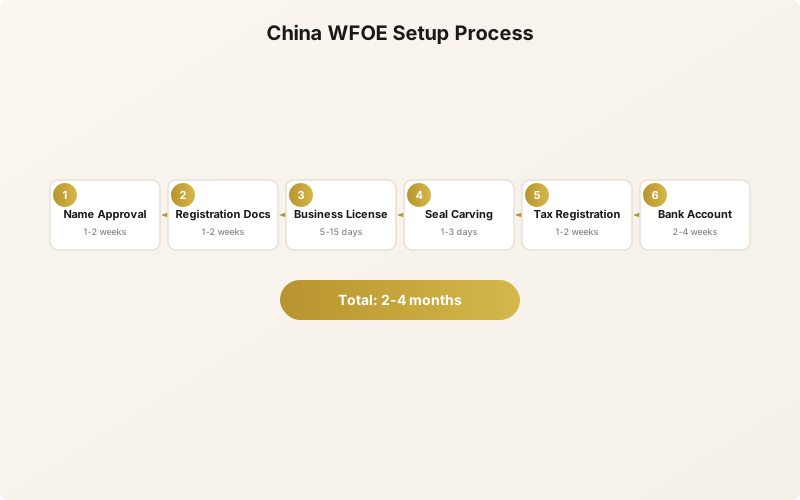
A2: The WFOE setup process typically takes 2-4 months from start to finish, depending on the industry and location. The timeline includes: name approval (1-2 weeks), preparing registration documents (1-2 weeks), business license application (5-15 business days), seal carving (1-3 days), tax registration (1-2 weeks), bank account opening (2-4 weeks), and any special industry licenses (variable timeline). Certain restricted industries may require additional approvals that can significantly extend the timeline.
Q3: What industries are restricted for foreign investment in China?
A3: China publishes a Foreign Investment Negative List that specifies industries where foreign investment is prohibited or restricted. Prohibited sectors include certain news media, compulsory education institutions, and some rare earth mining. Restricted sectors where foreign ownership is limited include telecommunications, education, healthcare, financial services, and agriculture. The negative list is periodically updated, generally becoming more open over time. Industries not on the negative list receive national treatment, meaning foreign investors enjoy the same treatment as domestic investors.
Q4: What is the minimum registered capital for a WFOE?
A4: China abolished the statutory minimum registered capital requirement for most industries in 2014 under the注册资本认缴登记制 (subscription system). However, companies must still specify a registered capital amount and contribution timeline in their articles of association. The practical registered capital amount should reflect the actual operational needs of the business and the industry norms. Some regulated industries still have minimum capital requirements, such as banking, insurance, securities, and certain types of consulting businesses.
Q5: What is the difference between a WFOE and a joint venture in China?
A5: A WFOE (Wholly Foreign-Owned Enterprise) is a limited liability company entirely owned by foreign investors, offering full control over operations but requiring the foreign investor to handle all aspects of market entry independently. A joint venture involves partnering with a Chinese shareholder, which can provide market access, local expertise, and government relationships but requires sharing control and profits. The choice depends on the industry (some sectors require joint ventures under the negative list), the level of local market knowledge needed, and the desired degree of operational control.
Further Reading
- China Product Certification: CCC, CQC, SRRC and More — A Complete Guide for Foreign Hardware Companies — Certification for electronic products
- Rapid Prototyping and Sampling in China: A Complete Guide for Hardware Startups — PCB prototyping and fast turns
- Product Assembly, Testing, and Final Inspection in China: A Complete Guide — PCBA assembly and testing
- Supply Chain Risk Management in China: A Practical Guide for Hardware Companies — PCB supply chain risks
Next Steps
For hardware teams, the legal questions follow the sourcing sequence: select and vet a factory, fix tooling and payment terms, then protect the design and manage inspection, certification and export. The guides below follow that sequence.
Two service lines most often relevant at this stage:
- Which contracts does an AI company need before selling in China?
- How can a foreign AI company protect its models and code in China?
To discuss scope, timeline and fees for your own matter, Contact Us About Your China Entry. The initial consultation is free; the form prepares an email in your own mail application.
Related guides in this series
- China Hardware & Supply Chain Guide for Foreign AI Companies
- How to Select and Vet Factories in China: A Complete Sourcing Guide for Hardware Startups
- Cost of Manufacturing in China: What Foreign Hardware Startups Should Budget
Frequently Asked Questions↑ Back to article
How much does PCB manufacturing cost in China?
PCB costs in China vary widely based on layer count, board size, quantity, and material. Prototype 2-layer FR-4 boards (10cm x 10cm, 10 pieces) typically cost $5–$20 total. 4-layer prototypes range from $15–$50 for 10 pieces. Volume production for 2-layer boards can be as low as $0.30–$1.50 per board at quantities of 1,000+, while 6–8 layer boards cost $2–$8 each. HDI and flex PCBs are significantly more expensive, often 2–5x the cost of standard FR-4 boards.
What is the typical lead time for PCBs in China?
Prototype PCBs in China can be turned around in 24–72 hours for simple 2–4 layer boards through fast-turn services. Small batch orders (50–500 pieces) usually take 5–7 days. Volume production (1,000+ pieces) typically requires 10–20 days depending on complexity. Lead times increase with layer count, special materials, surface finishes like ENIG, and factory backlog. PCBA adds 3–10 days on top of bare board lead time.
How do I choose a good PCB factory in China?
Look for factories with UL, ISO 9001, and RoHS certifications at minimum. For higher reliability products, seek IPC-6012 qualification. Evaluate their equipment age, quality systems, engineering support capability, and English communication. Always start with a sample or prototype run before committing to volume. For high-volume programs, plan a factory visit to audit capabilities. Match the factory tier to your needs — prototype shops for speed and low cost, mid-tier factories for balanced quality and price, and top-tier factories for demanding applications.
What are common PCB quality issues from Chinese factories?
Common PCB quality issues include solder bridging between pads, tombstoning of components during assembly, delamination of layers, misregistration (misaligned layers), via problems (voids, insufficient plating), uneven plating thickness, poor solder mask adhesion, and incorrect drill sizes. These issues are more common with lower-tier factories. Mitigation strategies include specifying IPC standards and AQL levels, requesting AOI and electrical testing, and conducting incoming inspection before accepting shipments.
What is the difference between PCB and PCBA?
PCB (Printed Circuit Board) refers to the bare board — the fiberglass or other substrate with copper traces, pads, and vias, but no electronic components mounted. PCBA (Printed Circuit Board Assembly) is the complete board with all components (ICs, resistors, capacitors, connectors, etc.) soldered onto the PCB. PCBA adds the SMT (Surface Mount Technology) or THT (Through-Hole Technology) assembly process, component sourcing, and testing on top of bare PCB manufacturing.
What types of PCBs can be manufactured in China?
China has comprehensive PCB manufacturing capabilities covering virtually all types. This includes single-layer and double-layer boards, multi-layer boards up to 30+ layers, HDI (High-Density Interconnect) boards with microvias, flexible PCBs (FPC) and rigid-flex boards, high-frequency boards for RF applications, metal-core PCBs for thermal management, and specialty boards for automotive, medical, and aerospace applications. China produces over 55% of the world's PCBs, offering unmatched scale, technology capability, and cost efficiency across the full range of board types.
What is DFM and why is it important for PCB manufacturing?
DFM (Design for Manufacturing) for PCBs is the process of optimizing your board design to ensure it can be manufactured reliably and cost-effectively. Good DFM includes following minimum trace width and spacing rules, proper annular ring sizes, adequate solder mask clearance, appropriate drill hole sizes, and design rules matched to your factory's capabilities. Good DFM reduces manufacturing defects, lowers costs, shortens lead times, and improves yield. Most Chinese PCB factories provide DFM checks as part of their quotation or order process, and addressing DFM issues early prevents costly delays and re-spins.